Intel 65nm and Beyond (or Below): IDF Day 2 Coverage
by Kristopher Kubicki on September 9, 2004 9:26 AM EST- Posted in
- Trade Shows
Next Generation Improvements
Of course, Montecito is already old news. 90nm is already old news. Strained silicon, low-k dialectrics and phase shifting lithography masks are also old news. Our interests belong to some of the technologies Intel discussed to bring the company out of the 90nm age in two years; into the 65nm interconnect era.
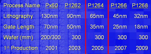
At AnandTech, we love roadmaps - particularly roadmaps with internal code names, wafer sizes and process technology. Stumbling into a development talk at the right time gave us a glimpse at Intel's 6 year plan for lithography.

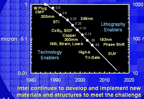
Intel positioned itself to ramp a new lithography generation every two years - currently the 90nm D1D in Hillsboro, Oregon, houses the development technologies for 2005's introduction of 65nm technology. Some of Intel's most promising technologies fit into a nice line graph plotting process size against time.

Technologies like strained silicon and low-k dialectrics are just first steps for Intel. We are going to give a small primer on as much of these technologies as possible.


21 Comments
View All Comments
mikecel79 - Thursday, September 9, 2004 - link
Great article on Intel's technology but why nothing about the dual core P4 they showed running on a 915 board yesterday?From the ZDnet article at http://zdnet.com.com/2100-1103_2-5356703.html
"Like the current Pentium 4, Intel's dual-core desktop chip is built on the NetBurst architecture and fits into motherboards using Intel's 915 Grantsdale chipset. But Siu declined to provide many details on the dual-core demonstration chip, which he described as an engineering prototype.
"It is real silicon running on a standard 915 platform," Siu said. He wouldn't comment on whether it has the 64-bit memory extension technology, called EM64T."