Intel Developer Forum Spring 2003 - Day 2: Prescott Info Galore
by Anand Lal Shimpi on February 19, 2003 1:56 PM EST- Posted in
- Trade Shows
One of the most important tracks to attend at IDF was one about IA32 Architecture Trends and Research, not only because it provides an insight into Intel's plans for upholding Moore's law for the next decade, but also because of a little gem called Prescott.
Intel's Prescott core will be their first CPU built on their new 90nm process, and is due out before the end of this year. We've talked about Prescott for a while, but Intel has finally disclosed all of the major pieces of information about the successor to the Northwood Pentium 4.

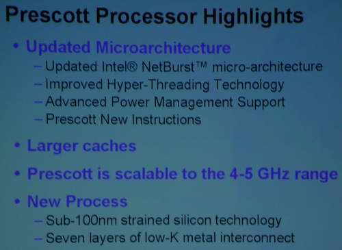
The slide above gives you an idea of the overall improvements to the Prescott core. The updated Intel NetBurst micro-architecture comes in the form of an 800MHz FSB and a larger L1 data cache of 16KB, up from the 8KB of the Willamette and Northwood cores.
The improved Hyper-Threading technology in Prescott comes in the form of two new Hyper-Threading specific instructions, that are a part of the 13 total new instructions that made it into Prescott.
We've been mentioning for a while that Prescott will feature a large 1MB L2 cache, and Intel has publicly confirmed this at IDF. The 1MB L2 cache will bring Prescott up to around 100 million transistors, rivaling some of the most complex GPUs in transistor count.
The 90nm process combined with additional enhancements to Intel's manufacturing processes will allow the Prescott core to scale to the 4 - 5GHz range before it will be replaced by Tejas, which we mentioned earlier today.
The 90nm strained silicon process is something we've talked about in the past, so be sure to check out our previous article on strained silicon to understand the benefits of the technology.


0 Comments
View All Comments